

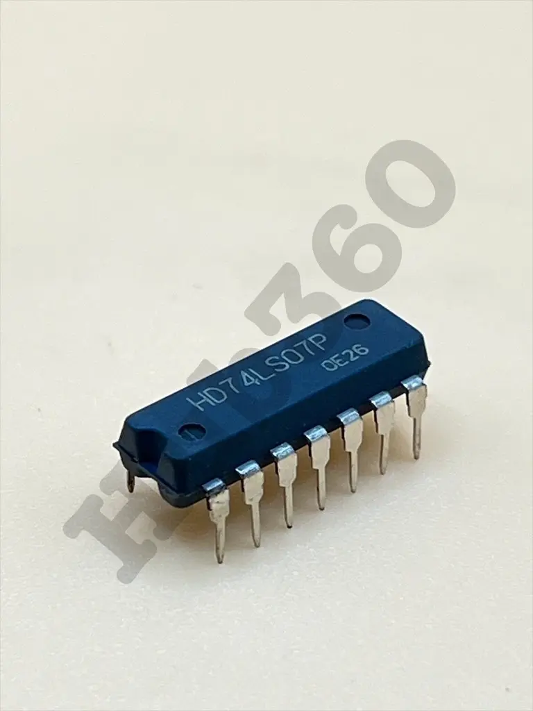
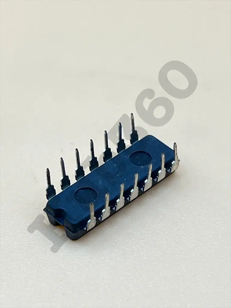


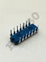
HD74LS07P (74LS07) logic chip
Description:
The HD74LS07P is a hex inverter buffer/driver with open-collector high-voltage outputs. It belongs to the LS family of high-speed Schottky TTL (Transistor-Transistor Logic) integrated circuits. This device features six independent inverters, each with an open-collector output stage. It is designed for interfacing and driving devices that require high voltage compatibility and can sink larger currents than typical TTL outputs.
Key Features:
- Hex inverter buffer/driver
- Open-collector outputs for high-voltage applications
- LS TTL (Low-Power Schottky Transistor-Transistor Logic) technology
- Wide operating voltage range: 4.75V to 5.25V
- High-speed operation
- Typical propagation delay: 10ns
- High output sink capability: 20mA (min)
- Standard 14-pin DIP (Dual In-line Package) package
- Package Type: 14-pin DIP
- Supply Voltage (V_CC): 4.75V to 5.25V
- Input Voltage (V_IN): 0V to V_CC
- Output Voltage (V_OUT): 0V to 30V
- Input High Voltage (V_IH): 2V (minimum)
- Input Low Voltage (V_IL): 0.8V (maximum)
- Output Current (I_O): 20mA (minimum)
- Quiescent Supply Current (I_CC): 8mA (maximum per gate)
- Propagation Delay Time: 10ns (typical)
- Operating Temperature Range: 0°C to +70°C
- Logic Level Shifting: Converting between different logic voltage levels.
- Signal Inversion: Inverting logic signals for complementary logic operations.
- Bus Interface: Driving and buffering bus lines in digital systems.
- Pulse Shaping: Forming and modifying pulse signals in digital circuits.
No Specifications